Fredys Matos Borges, PCB Design Engineer specializing in IoT and embedded systems, based in Havana, Cuba
Automation Control Engineer

FREDYS MATOS BORGES

Professional PCB Design & Review for IoT and Embedded Systems

I help engineers and startups design and validate IoT hardware from concept to production-ready PCB.

Request a PCB Design Quote
15+
PCB Designs
98%
First-Pass Success
8
Layer Max

Professional PCB Design & Review Services

I specialize in designing and reviewing PCB layouts for IoT and embedded devices — helping startups, makers, and engineers reduce risk, improve manufacturability, and bring products to market faster with zero-defect manufacturing.

PCB DESIGN (Full Service)

  • Schematic capture with professional symbol libraries
  • Multi-layer PCB layout (up to 8 layers) with HDI support
  • Design for Manufacturability (DFM) validation
  • Comprehensive BOM with sourcing alternatives
  • Fabrication-ready files (Gerber, ODB++, Pick & Place)

Delivery time (typical)

Simple design: 5–10 business days

Complex design: 10–20+ business days

Price range

Simple boards: $250–$500

Moderate/complex: $500–$900+
Request PCB Design

PCB DESIGN Review & Optimization

  • Schematic functionality review
  • Signal & power integrity analysis
  • DFM/DFA audit using real manufacturer rules
  • Thermal and EMI compliance check
  • Clear improvement roadmap with annotations

Delivery time (typical)

2–4 business days

Price

$80–$120

Request Design Review

Who I Work With

Technologies & Tools

Every design undergoes rigorous validation against IPC-2221, IPC-7351, and real-world DFM rules. My PCBs are optimized for high-yield manufacturing.

IPC Compliant
RoHS/REACH
CE/EMC Ready

My Engineering Process

A structured, battle-tested approach that minimizes risk and ensures manufacturing-ready results.

1

Requirements & Architecture

Define system specs, power, comms, environment, and create block diagrams.

2

Schematic Design

Professional schematics with proper net naming, power planning, and component selection.

3

PCB Layout

Precision routing with focus on signal/power integrity, thermal, EMI, and DFM.

4

Review & Optimization

Full validation: crosstalk, return paths, power delivery, thermal, DFM/DFA.

5

Deliverables

Gerber, ODB++, BOM, assembly drawings, test docs — ready for manufacturing.

Featured Projects

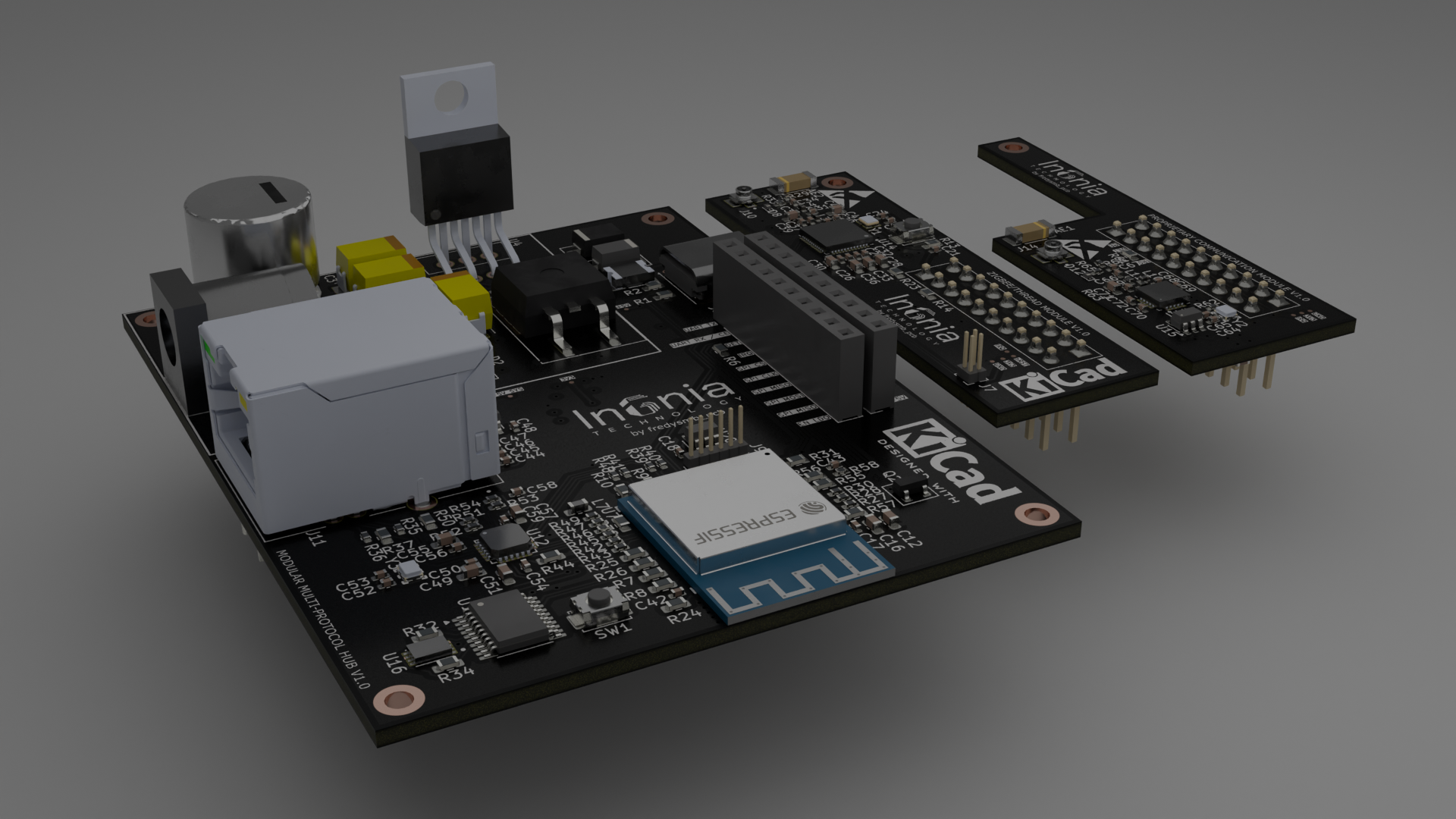
3D render of Modular Multi-Protocol IoT Hub PCB with ESP32-S3, Zigbee, Thread, and Ethernet interfaces
IoT Gateway

Modular Multi Protocol Hub

ESP32-S3 Zigbee Thread Ethernet

Industrial IoT gateway with modular radios, isolated power, battery backup, and full EMI shielding.

View Project
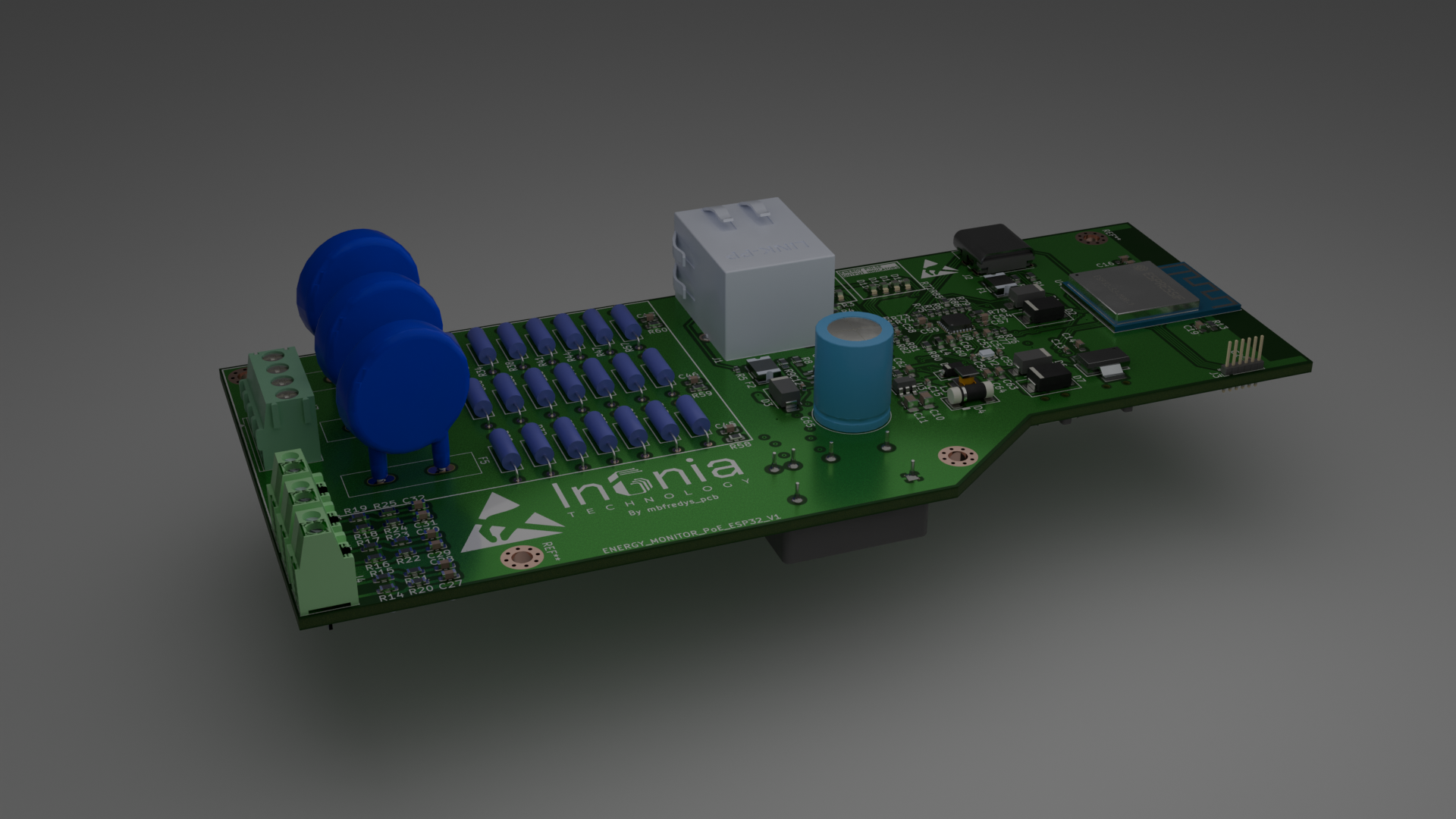
3D model of 3-Phase Energy Monitor PCB for building management systems with ESP32-S3 and ATM90E32 sensor
Smart Building

3 Phase Energy Monitor

ESP32-S3 PoE ATM90E32 Isolation

Energy monitoring for BMS with 3-phase measurement, full isolation, PoE, and industrial protection.

View Project
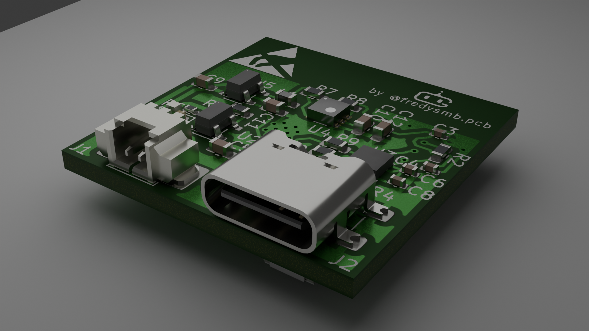
3D visualization of Mini Environmental Sensor PCB with ESP32-C3, BME280, and SPG40 air quality sensors
Sensors

Mini Environmental Sensor

ESP32-C3 BME280 SPG40 Li-Po

Battery-powered environmental monitor with multi-sensor air quality, cloud connectivity, and power management.

View Project

Start Your Hardware Project

Ready to bring your IoT or embedded hardware to life? Let's discuss your requirements.

Your data is used solely to respond to your inquiry. I do not share your information with third parties. Messages are stored securely and deleted after project completion.

Based in Havana, Cuba | Global Remote Collaboration

All communications are treated with professional confidentiality